Numerical Simulation for Cd-free Sb2S3 based Photovoltaics
Main Article Content
Article Sidebar
Abstract
Solar energy harnessing can meet energy demand of the world and can solve the problem like global warming caused by traditional source fossil fuel. Photovoltaic technologies including wafer, thin film, and organic solar cell have been developed to convert solar energy into electricity. Among them, thin film technology needs very less material to fabricate the solar cell which makes thin film solar cell cost effective and more available in the market. CIGS (Copper Indium Gallium Selenide) and CdTe (Cadmium Telluride) based solar cells are commercially available thin film solar cells since it has got efficiency comparable to silicon wafer solar cells. But due to the scarcity of the constituent elements like In, Ga and toxicity of Cd hinder further development. CZTS (Copper Zinc Tin Sulfide) solar cell made of earth abundant material was believed to overcome scarcity and toxicity issue but the associated secondary phases result in low efficiency [1].
On searching alternative material for thin film technology, antimony sulfide Sb2S3 deserves special attention due to its suitable optoelectronic properties including band gap (1.7eV) and high absorption coefficient ( > 104 cm-1), stable phase, and non-toxicity [2]. Recently, Sb2S3 is being widely studied for its photovoltaic property and has emerged as a suitable alternate to the quaternary CIGS and CZTS based photovoltaics (PV). Despite numerous research work focused on antimony sulfide, its power conversion efficiency is still low and is limited to ~7% [3]. The low efficiency can be attributed to quick recombination of electron and hole due to the presence of mid-gap as well as interfacial defects. Another major challenge in Sb2S3 based PV is the band offset between the absorber and the buffer layers. Conduction band offset (CBO) strongly influences the photoconversion efficiency [4]. CdS is the conventional buffer layer in CIGS and CZTS photovoltaic cells and the same also has been reported widely for Sb2S3. The CBO for Sb2S3/CdS heterojunction is nominal with a spike of ~0.37 eV. But, the usage of cadmium is not environment friendly for both producer and consumer. Further, the narrow band gap of CdS causes absorption at shorter wavelength region and reduces the overall efficiency [5]. Keeping this we propose a suitable alternative ternary buffer layer Zn(O,S) for Sb2S3 PV cell for which the CBO can be tuned by varying the S concentration.
In the present work, Sb2S3 PV cell with Zn(O,S) buffer layer has been numerically analyzed using SCAPS 1D [6] simulator. SCAPS 1D calculates solar cell parameter using Poisson’s equation and continuity equation for hole and electron. Simulation has been carried out for the solar cell configuration ITO/Zn(O,S)/Sb2S3/Ni. Zn(O,S) has been used as buffer layer to overcome the issue connected with traditional CdS buffer. The electron affinity of Zn(O,S) can be tuned by varying the S content which in turn enables the tuning of CBO. The simulation is performed in two stages. Firstly, absorber layer thickness, buffer layer thickness, carrier concentration, defect density and interface defect density are optimized. The electron affinity of buffer layer is optimized to optimize the CBO between the absorber and the buffer layers. Secondly, under optimized condition, the solar cell ITO/Zn(O,S)/Sb2S3/Ni is simulated. The solar cell parameter such as open circuit voltage (Voc), short circuit current density (Jsc), fill factor (FF) and power conversion efficiency have been obtained under global AM 1.5 conditions. The main objectives of the present work are to find the optimal layers parameters for achieving better efficiency and to replace the toxic CdS with Zn(O,S). This work will serve the experimentalist to overcome difficulties associates with Sb2S3 solar cell and it will also provide a direction to improve efficiency of the solar cell. Figure 1 shows the proposed structure of the solar cell and Figure 2 shows the J-V characteristic result of the SCAPS for the structure. Device layer parameters used for simulation have been mentioned in Table 1.
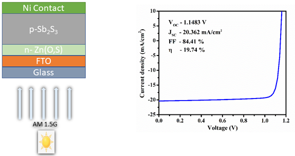
Fig.1. Proposed solar cell structure Fig.2. Initial J-V characteristic result
Table 1: Layer parameters for Sb2S3/Zn(O,S) solar cell simulation using SCAPS-1D
Material Parameters
FTO
Zn(O,S)
Sb2S3
Thickness (mm)
0.5
0.1
1
Bandgap (eV)
3.5
2.83
1.7
Electron Affinity (eV)
4
3.6
3.7
Dielectric Permittivity
9
9
7.08
CB Effective Density of State (1/cm3)
2.2 x 10¹⁸
2.2 x 10¹⁸
2.2 x 10¹⁹
VB Effective Density of State (1/cm3)
1.8 x 10¹⁹
1.8 x 10¹⁹
1 x 10¹⁹
Electron Thermal Velocity (cm/s)
107
107
107
Hole Thermal Velocity (cm/s)
107
107
107
Electron Mobility (cm2/V.s)
20
100
20
Hole Mobility (cm2/V.s)
10
25
10
Donor Density (ND) (cm-3)
1020
2 x 10¹⁶
0
Acceptor Density (NA) (cm‑3)
0
0
5.5 x 10¹⁵
How to Cite
Article Details
Simulation, Antimony sulfide, Zincoxysulfide, Buffer layer, SCAPS 1D, Optimization
[1] Hongwei Lei, Jianjun Chen, Zuojun Tan, Guojia Fang, Solar RRL, 3, 1900026, 2019.
https://doi.org/10201900026.1002/solr.
[2] Rokas Kondrotas, Chao Chen,Jiang Tang, Joule, 2, 5, 2018.
https://doi.org/10.1016/j.joule.2018.04.003
[3] Yong Chan Choi, Dong Uk Lee, Jun Hong Noh, Eun Kyu Kim,Sang Il Seok, Material Views, 24,23, 2014
https://doi.org/10.1002/adfm.201304238
[4] Dong Gwon Moon, Shanza Rehan, Deuk Ho Yeon, Seung Min Lee, Sun Jae Park, SeJin Ahn, Yong Soo Cho, Solar Energy Materials and Solar Cells, 200, 109963, 2019.
https://doi.org/10.1016/j.solmat.2019.109963
[5] Kuldeep S Gour ,Rahul Parmar, Rahul Kumar, Vidya N Singh, A journal of Nanoscience Nanotechnology, 6, 20,2020.
https://doi.org/10.1166/jnn.2020.17537
[6] Marc Burgelman, Koen Decock, Samira Khelifi, Aimi Abass, Thin Solid Films, 535, 2013.
https://doi.org/10.1016/j.tsf.2012.10.032