Ab initio calculations on Zn(O,S) buffer layer for cost effective photovoltaics
Main Article Content
Article Sidebar

Abstract
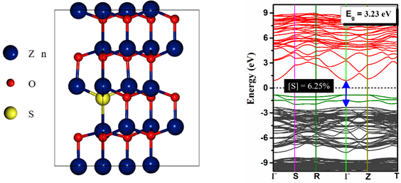
Zinc oxysulphide (Zn(O,S) is a promising material for replacing the Cd-free buffer layer in thin film photovoltaic (PV) cell. This material has sparked a lot of interest because of its wide bandgap tunability by varying the sulphur and oxygen concentrations [1-2]. Furthermore, at higher sulphur concentrations (S > 70%), Zn(O,S) has an ideal conduction band offset with Cu2O which is an earth abundant and environment friendly absorber layer [3]. But, there are only limited studies which explain the optoelectronic properties of Zn(O,S) system in terms of its electronic density of states and band structure. Therefore in the present work, we have studied the optoelectronic properties of Zn(O,S) for O rich (hexagonal wurtzite phase) as well as S rich (cubic zinc blende phase) conditions through ab initio calculations. The density functional theory calculations were performed using the plane wave self-consistent field (PWSCF) approach as implemented in the Quantum ESPRESSO package [4]. The interactions between the core electrons and the valence electrons were represented by the projector augmented wave (PAW) method. Generalized gradient approximation (GGA) as parametrized by Perdew-Burke-Ernzerhof (PBE) was used to treat the electron exchange and correlation terms. For the hexagonal wurtzite structure, the 2 \times 2 \times 2 supercell of ZnO containing 32 atoms was created in which S was introduced as the anionic substitutional impurity (Fig. 1a). On the other hand, the 2 \times 2 \times 2 supercell of zinc blende ZnS contains 64 atoms in which O was introduced as the anionic substitutional impurity. The undoped as well as the doped structures were fully relaxed in terms of their atomic coordinates and cell dimensions. The total energy during was converged to within 10-8 Ry. The semi-empirical DFT+U (Hubbard-U correction) calculations were performed to take into account the correlation effects in ZnO and ZnS. Fig. 1a, b shows the optimized crystal structure with the calculated electronic band structure for S doped ZnO system. For pure ZnO, the lattice parameters were found to be a = b = 3.2786 Å and c = 5.2941 Å which is in accordance with the reported values in the literature. S doping resulted in an increase in the lattice volume with the corresponding lattice parameters as a = b = 3.3121 Å and c = 5.3547 Å. The electronic band structure clearly indicates the semiconducting nature for ZnO as well as S doped ZnO with a direct band gap at the -point. The direct band gap was found to be slightly increased from 3.06 eV to 3.23 eV with S incorporation into the hexagonal lattice. From the band structure, substitutional S was found to be acting as a donor with the corresponding defect levels lying below the Fermi level. Similarly, the electronic density of states (DOS) also reveals the presence of S related impurity states at the forbidden region. Based on the ab initio calculations, the proposed Cu2O based PV cell with Cu2O/Zn(O,S)/Al:ZnO device structure was simulated under AM1.5 conditions by using the SCAPS-1D software [5]. The efficiency (η), fill factor (FF), short-circuit current density (JSC), and open-circuit voltage (VOC) were calculated at various thicknesses of the Zn(O,S) buffer layer. Besides this, we also examined the quantum efficiency for the proposed device. The ab initio calculation as well as the device simulation performed in the present study will help the experimentalists to design the cost-effective Cu2O based PV cell with enhanced photoconversion efficiency.
(a) (b)
Fig.1. (a) Optimized crystal structure for S doped ZnO and (b) Electronic band structure for S doped ZnO across the high symmetry k-points
How to Cite
Article Details
Zinc oxysulphide, Buffer layer, Ab initio, Photovoltaics, Doping, Band structure, Simulation
https://doi.org/10.1063/1.4820383
[2] Y.Z. Yoo, Z.W. Jin et al., Appl. Phys. Lett. 81(2002) 3798-3800.
https://doi.org/10.1063/1.1521577
[3] Riley E. Brandt, Matthew Young et al., Appl. Phys. Lett.,105, 263901 (2014).
http://dx.doi.org/10.1063/1.4905180
[4] P. Giannozzi, S Baroni et al., J. Phys. Condens. Matter 21 (2009), 395502-1-19.
https://doi.org/10.1088/0953-8984/21/39/395502
[5] M. Burgelman, P. Nollet et al., Thin Solid Films 361 (2000) 527–532.
https://doi.org/10.1016/S0040-6090(99)00825-1